7
$\begingroup$

I'm in the process of building a RF buffer-amplifier chain for a VFO and I'm experiencing a design issue trying to impedance match between the sections.

The issue I'm having is that many (most) of the circuit designs documented are characterized with a source or load impedance of 50 ohms. Lets take the following snippet as an example:

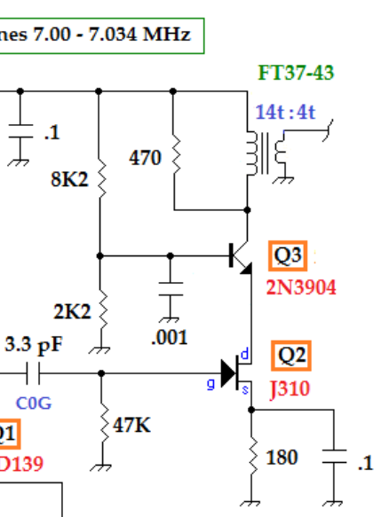
Vackar Buffer Amp

Taken from here pg. 520. I've prototyped this buffer amp at 50 MHz and works quite nicely. It gives a gain of just over 3 and a power output of ~12dBm. But, the key point is that all of these characteristics are based on a reflected collector impedance of ~260 ohms and assume a 50 ohm load.

Now, I'd like to follow this pre-amplifier with a power amp and many of the examples I'd like to prototype have an impedance transformer at the input. Something like the following is very common:

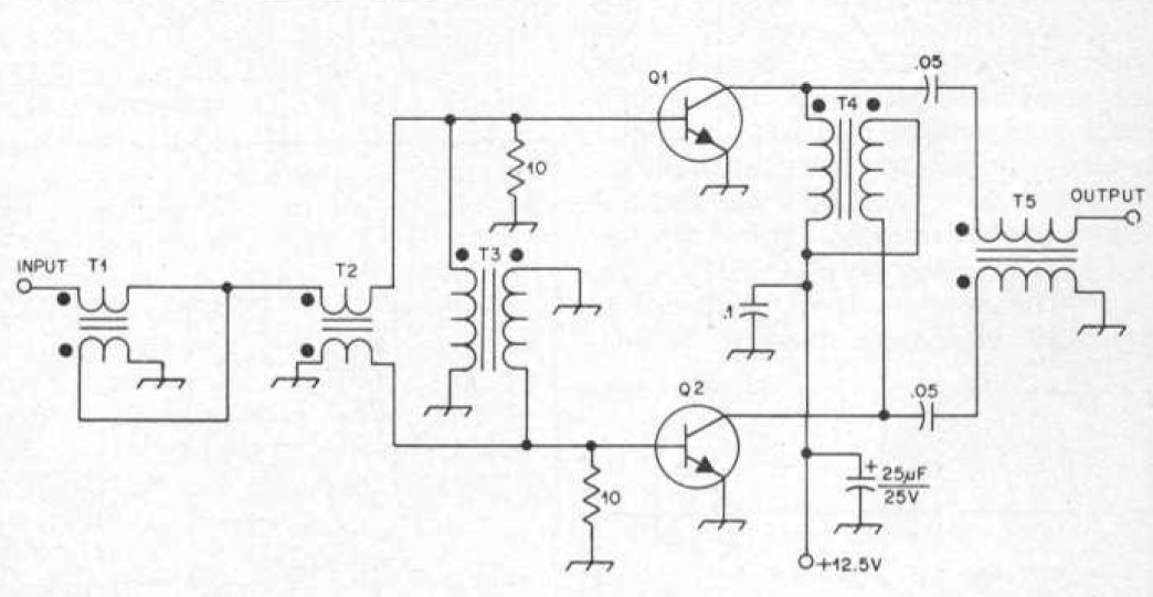
RF Power Amplifier

And again, the amplifier is documented assuming the signal generator at the input has a 50 ohm output impedance.

In my case, I would like to combine these two amplifiers into a pre-amp and power amp chain. The obvious solution is to combine the transformers into a single transformer that presents ~260 ohms to the collector of the pre-amp and ~6 ohms at the base of each power transistor base (in the power amplifier shown T1 is a 4:1 impedance transformer => 50 ohms becomes 12.5 and each base sees half of that).

But, I've lost my fixed 50 ohm impedance. If I combine the transformers I make the collector load of the pre-amp directly dependent on the RF input impedance of the power amp transistors (which is nearly always a complex quantity and is non-trivial to measure).

So, I'd like to know if there are any "tricks" to pin the inter-stage impedance to a particular value or is there nothing for it but to characterize the input impedance of the power amp?
$\endgroup$

4 Answers 4

6
$\begingroup$

There is no need to "pin" an interstage impedance. You may directly transform from the native output impedance of one stage to the native input impedance of the next without going through an intermediate transformation or termination.

When designing an interstage transformer, the general design rule is to ensure that the inductive reactance of each winding is at least 10 times the impedance to which it is connected. This ensures that the transformer winding impedance does not swamp out the attached impedance.

Also take care to think through the transformer topology. Take note that the first circuit uses isolated windings for the output transformer while the second circuit uses an autotransformer at its input stage. The combined impedance transformation will require isolated windings so as to restore a ground referenced output of the previous stage.

$\endgroup$
3
$\begingroup$

T1 in the "power amp" schematic you provided is a 4:1 step down transformer. Its purpose is to match - that is, maximize power transfer between - the preceding stage and the power amp transistors, whose high impedance is "swamped" by the 10-ohm resistors.

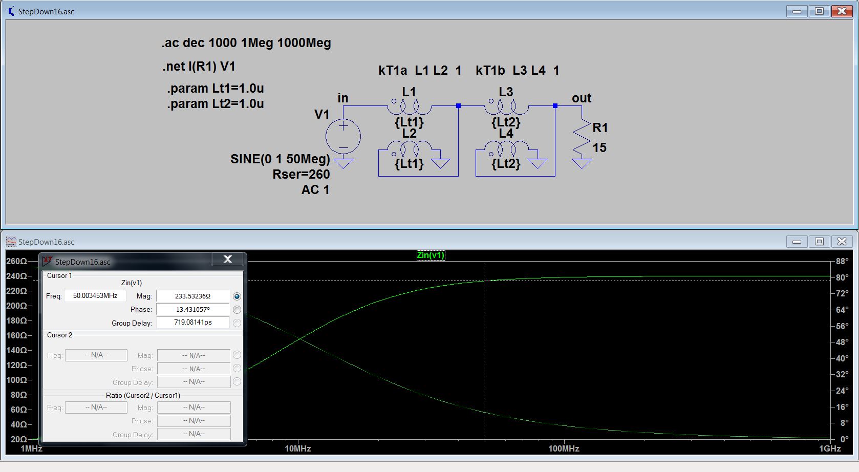
You can match the ~260-ohm driver to the PA by replacing T1 with a 16:1 step down transformer and replacing the 10-ohm resistors with 15-ohm resistors. You might find it simplest to accomplish the higher step down ratio by adding a second "copy" of T1 between the input and T2. Simulation indicates that an inductance of 1-uH should suffice for each of the four windings on T1a and T1b:

enter image description here

$\endgroup$
0
$\begingroup$

(most) of the circuit designs documented are characterized with a source or load impedance of 50 ohms.

True, but not important. In order to match impedence, the output impedance of the previous stage should match the input impedance of the next stage. That's all you need. Using bipolar transistors, for example, the output impedance is approximately equal to the collector resistor. The input impedance is roughly equal to beta times the emitter resistor, if not bypassed.

building a RF buffer-amplifier chain for a VFO

Therefore, if building a buffer, you don't need to match impedances, but just to lightly load the oscillator. Just the opposite of matching.

$\endgroup$
0
$\begingroup$

Your power amp is a push-pull, meaning the output power is meant to be at least a few Watts, and the input must be fairly strong to drive that class-C amp.

Your J310 cascode preamp is meant for a receiver preamp or possibly an IF amp rather than a transmitter driver amp. That amplifier will not produce an output power sufficient to drive that power amp, regardless of the impedance matching. This amplifier can be used as a buffer amp following the VFO quite well, but it may be an overkill. You'll need at least one more stage to a level where you can drive a class-C power amp.

Now, interstage matching is not an exact "matching" like matching a load over a transmission line. The collector or drain output impedance is not a definitive number, and it varies based on the power level, the supply voltage, the level of distortion tolerated, and whether you want to maximize the gain, power efficiency, or stability. As you see, it is a trade-off. The base/gate driving impedance is better defined, measured, and matched but still subject to similar trade-offs. (For example, the base/gate is often matched to achieve minimum noise figure rather than maximum gain at the receiver frontend.)

Also, the way FT37-43 is wound in the preamp is suitable for up to 10MHz range, but I would choose a Ruthroff transformer configuration if you operate it at 50MHz.

With all the above combined, the best way to match between those two amplifiers is another amplifier stage to meet the required power level and the impedance. Both amplifiers are broadband amps, so having another broadband amp as the drive stage makes sense. The most common matching option is Ruthroff transformers, and you can use one transformer to match the collector to the next stage's base.

Incidentally, if you are making a single-band transmitter, building the entire amplifier chain in a narrowband design makes sense. In that case, the interstage matching can be done with one of several types of LC networks. Narrowband design typically yields more gain, power efficiency, and lower harmonics.

$\endgroup$

You must log in to answer this question.

Not the answer you're looking for? Browse other questions tagged .