9
$\begingroup$

Firstly, feel free to move this to Electronics SE if it's not on-topic, but it's strongly related to ham radio and RF circuitry.

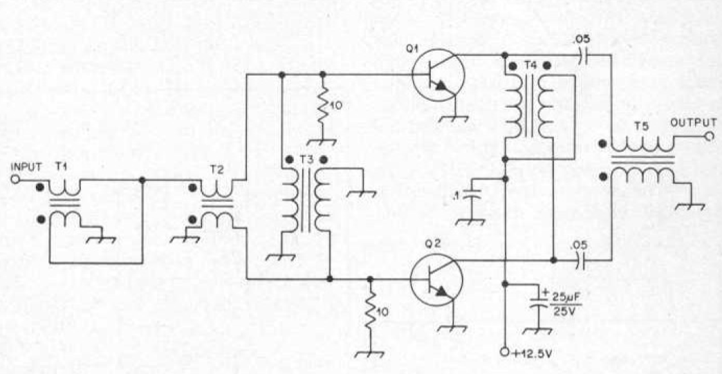
Reading Hayward's classic "Solid State Design for the Radio Amateur" and looking for inspiration, I came across the following push-pull PA design that I didn't quite understand (Chapter 4, Pg 62).

enter image description here

I don't have a problem with T1 and T2, it's T3 and T4 I'm struggling with. T1 is a straightforward 4:1 impedance transformer; it doubles the current at the output and so "looking back into" T1 the source appears to have 4 times less impedance. No problems there. T2 has the dotted secondary tied to ground and so the current flowing into the dot (transformer action) leaves the other end of the secondary negative. Now we have anti-phase signals of equal amplitude at the transistor bases, turning each transistor on and off alternately. Again no problems there, it's straightforward push-pull action.

But here's where the wheels fall off for me! What's the purpose of T3 (and T4 which I believe has a similar purpose)? Here's what the author says: "The third core [in the input section of the amplifier] ensures that the load presented to T2 is balanced. Each transistor sees a driving impedance of 6.25 ohms". I've included a hand-sketched re-arrangment of the circuit to help me understand and I can sort of see how the current produced by the full potential of the balanced signal (anti-phase peak-to-peak) is driven through one or other transistor bases. Does this account for the halving of impedance "seen" by each transistor as the author says? But then, wouldn't this happen anyway, without T3??
enter image description here

$\endgroup$

2 Answers 2

6
$\begingroup$

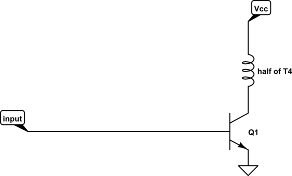
T4 is just this idea:

schematic

simulate this circuit – Schematic created using CircuitLab

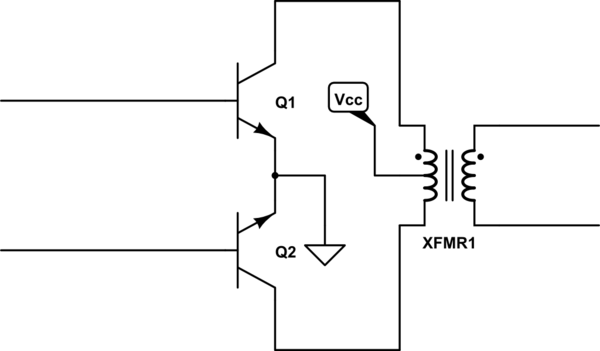
Sometimes it's done this way:

schematic

simulate this circuit

The primary of XFMR1 is equivalent to T4 from the question.

Since T4 provides the collector load for the transistors, it's a factor in voltage gain. For a differential-mode input, the collector currents correspond to magnetic flux in the same direction in T4, thus T4 presents a high impedance and voltage gain is maximized. For undesirable common-mode input (which could come from dissimilar gain in the transistors), magnetic flux cancels and T4 looks like a short to Vcc, minimizing voltage gain.

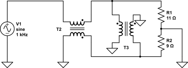
You're right T3 isn't ideally necessary, but it serves to keep things balanced despite variation in components. Consider a simplified case where the load is just a pair of 10 ohm resistors that might vary by +/- 10%:

schematic

simulate this circuit

T2 (ideally) requires that the current is equal in each of the windings, but since the resistors are not equal, the voltages across the resistors are not equal. The addition of T3 remedies the situation: in the common mode it appears as a short to ground. Thus, at the right side of T2 there will always be equal but opposite currents and voltages. Or as the author puts it, T3 "ensures that the load presented to T2 is balanced".

$\endgroup$
3
  • $\begingroup$ That's exactly what I was looking for Phil. Thankyou! Just to clarify, in the final paragraph when you refer to common-mode I take it you mean any part of the signal that isn't balanced or anti-phase? So, currents flowing against each other (as they would in anti-phase signals) present a high impedance, whereas other (imbalanced) parts of the signal are simply shunted to ground. Have I got that right? $\endgroup$
    – Buck8pe
    Commented Sep 11, 2018 at 21:59
  • $\begingroup$ @Buck8pe Sounds like you have the right idea. For circuits like this, it can be useful to think not of "what's going on in the top / what's going on in the bottom" but rather "what's going on with equal but opposite things / what's going on when the things are equal in both sides". For a linear circuit, you can break things down either way an analyze them separately, and then add them together to get the full picture. $\endgroup$ Commented Sep 11, 2018 at 22:05
  • $\begingroup$ That's spectacular Phil, I must have spent 2 days spinning my wheels looking at sims and wondering "why" it worked. That common mode comment has finally clinched it for me (and I can rest!) $\endgroup$
    – Buck8pe
    Commented Sep 11, 2018 at 22:08
3
$\begingroup$

T4 is the collector DC feed transformer. The inductance of each side of the transformer acts as an RF choke at the amplifier's operating frequency. The antiphase connection of the windings prevents DC saturation of the core material.

By coupling the currents in the bases of Q1 and Q2, T3 is a lossless means to compensate for the wide variation in transistor parameters that are to be expected. This reduces distortion and improves stability.

$\endgroup$
1
  • $\begingroup$ "The antiphase connection of the windings prevents DC saturation of the core material." is not the full story - or two rod chokes would suffice, one each side, but if you do try this the harmonics and efficiency are much worse than with this transformer arrangement. For efficiency you need class B - so as one transistor is pulling current the other should be fully off - but you need the collector voltages to be equal and opposite not one half-sine wave and one flat line - this transformer generates the matching 'up'collector voltage above the supply, as the other transistor conducts and pulls $\endgroup$
    – mike G7VZY
    Commented Aug 6, 2020 at 23:13

You must log in to answer this question.

Not the answer you're looking for? Browse other questions tagged .